

Most Popular Products


 Send Inquiry
PCB Design Service
Price 500 INR/ Unit
MOQ : 1 Unit
PCB Design Service Specification
- Layer Count
- Up to 12 Layers
- Minimum Hole Size
- 0.2 mm
- Prototype Support
- Available
- Material Used
- FR4, CEM1, CEM3, Aluminum
- After-Sales Support
- Comprehensive technical assistance
- Minimum Track Width
- 0.1 mm
- Type of PCB Design
- Single Side, Double Side, Multilayer
- Service Mode
- Online/Offline
- Service Location/City
- All Over India
- Supported File Formats
- Gerber, DXF, ODB++
- Testing Services
- Design Rule Check (DRC), Electrical Testing
- Feature
- Custom Design Layouts, Schematic Capture, PCB Prototyping
- Mounting Technology Supported
- Surface Mount Technology (SMT), Through Hole Technology (THT)
- Industry Served
- Electronics, Telecommunication, Automotive, Industrial Automation
- Design Software Used
- Altium Designer, OrCAD, Eagle, KiCAD, Allegro
- Turnaround Time
- 1-4 Weeks
- Impedance Control
- Available
- Confidentiality Agreement
- Offered upon request
PCB Design Service Trade Information
- Minimum Order Quantity
- 1 Unit
- Delivery Time
- 7 Days
About PCB Design Service
Experience sizzling innovation with our PCB Design Service, where fresh concepts meet peerless execution. Leveraging a towering array of capabilities-minimum track width of 0.1 mm, minimum hole size of 0.2 mm, and support for leading file formats like Gerber, DXF, and ODB++-we serve eminent clients across electronics, telecommunication, automotive, and automation industries. Whether you desire single, double-sided, or multilayer PCBs up to 12 layers, our experts ensure custom layouts, impedance control, DRC, and robust after-sales technical support. Add to Cart now for prompt delivery across India!
Directions of Use and Application Areas
Our PCB Design Service is straightforward to leverage: simply share your schematic files through our online or offline service modes. Ideal for electronics, telecommunication, automotive, and industrial automation, this offering integrates seamlessly with devices using SMT or THT mounting. Application media cover both hardware prototypes and production-level assemblies. Incorporating FR4, CEM1, CEM3, or Aluminum materials, our design process ensures optimal results for projects requiring reliability in performance-critical environments.
Packaging, Certifications, and Sample Options
Each PCB design is meticulously packaged with comprehensive documentation and testing reports. Certification standards such as ISO and RoHS compliance underline our market value and your product's credibility. We cater to sample requests before a finalized order, allowing you to assess and negotiate the proposal amount or asking price. Our transparent approach ensures every detail-right from quotation to delivery-reflects the standards of an eminent manufacturer and supplier in India's PCB design market.
FAQ's of PCB Design Service:
Q: How does the PCB design process work with your service?
A: After you submit your project details and files in supported formats like Gerber, DXF, or ODB++, our engineering team reviews requirements, initiates schematic capture, and develops custom layouts. Design Rule Checks (DRC) and electrical testing are performed before prototype delivery. Throughout, you receive technical support and clear communication.Q: What industries can benefit from this PCB Design Service?
A: Our PCB Design Service is tailored for electronics, telecommunications, automotive, and industrial automation sectors. We design for both high-volume production and prototype needs, catering to diverse application requirements within these industries.Q: When can I expect to receive my finished PCB design?
A: Turnaround times vary based on project complexity. Typically, designs are delivered within 1 to 4 weeks. We provide timelines upfront based on your specifications and prototype requirements.Q: Where is the PCB Design Service available?
A: Our design solutions are offered all over India, with support for both online and offline service modes. This ensures accessibility and convenience wherever your project is located.Q: What are the benefits of choosing your PCB Design Service?
A: Clients enjoy comprehensive design customization with minimum track widths, multilayer support, and impedance control. Our confidentiality agreements uphold your intellectual property, while certified quality standards, after-sales support, and sample options ensure reliability and satisfaction.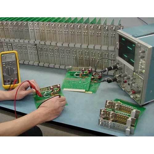
Tell us about your requirement

Price:
Quantity
Select Unit
- 50
- 100
- 200
- 250
- 500
- 1000+
Additional detail
Mobile number
Email

Quick Inquiry


Contact Details
GST : 27AAECJ1932H1ZO
S.No. 28/27, Near Eureka Internaionl School Pari Company Chowk, Narhe Dhayari Road,Pune - 411041, Maharashtra, India
Phone :07971645271

 |
JUSTGROW TECHNOLOGIES PRIVATE LIMITED
All Rights Reserved.(Terms of Use) Developed and Managed by Infocom Network Private Limited. |
